Scott Schrage, February 2, 2024
New material design for transistors could downsize next-gen tech
By better taming the Jekyll-and-Hyde nature of an alternative to the semiconductor — one that transitions from electricity-resisting insulator to current-conducting metal — Nebraska’s Xia Hong and colleagues may have unlocked a new path to smaller, more efficient digital devices.
The semiconductor’s ability to conduct electricity in the Goldilocks zone — poorer than a metal, better than an insulator — positioned it as the just-right choice for engineers looking to build transistors, the tiny on-off switches that encode the 1s and 0s of binary. Apply some voltage to the control knob known as a gate insulator, and the semiconductor channel allows electric current to flow (1); remove it, and that flow ceases (0).
Millions of those nanoscopic, semiconductor-based transistors now coat modern microchips, switching on and off to collectively process or store data. But as minuscule as the transistors already are, the demands of consumers and competition continue pushing electrical engineers to shrink them even further, either for the sake of squeezing in more functionality or downsizing the devices that house them. Unfortunately, those engineers are now bumping up against the practical and even fundamental limits of just how small semiconductors can get.
Researchers, in turn, have begun looking beyond not just industry favorite silicon but semiconductors as a whole. More than two decades ago, some began tooling around with a class of materials called Mott insulators. If the semiconductor is the happy medium that has driven decades of clockwork-constant progress, the Mott insulator is more akin to a two-faced wild card whose ambivalence rates as both the source of its appeal and of frustration.
A longstanding theory of conductivity says that a material with the electronic characteristics of a Mott insulator should generally be classified as a metal. Unlike the electrons in a metal or semiconductor, though, those in a Mott insulator don’t behave like independent particles. Instead, they interact in ways that confine them to localized sites and keep them from moving freely through a material. Still, certain conditions — higher temperatures, the introduction of more electrons — can overwhelm those forces, ultimately freeing the electrons and essentially transforming the Mott insulator into a conductive metal.
“So you (traditionally) have either itinerant electrons or localized electrons,” said Hong, professor of physics at the University of Nebraska–Lincoln. “It’s very clearly defined.
“But in the case of a Mott insulator, electron interactions cannot be ignored. Because of that correlation, it’s hard to define it as simply a metal or insulator. If you can tune the strength of the interaction, it can be a metal, or it can be an insulator.”
By topping a Mott insulator with a gate insulator made of so-called ferroelectric material — then using voltage to flip the latter’s polarization, or alignment of positive and negative charges — researchers realized they could direct the Mott transition from insulator to metal and back again. In that way, the pairing’s behavior, and most promising function, took after that of the semiconductor.
Yet the metallic phase of the Mott insulator lends it a vital advantage over its long-reigning counterpart: carrying a number and density of electric charges that far surpasses what a semiconductor ever could. The higher that density, the less space that charged electrons require to screen out electric fields that otherwise switch back the polarization of the ferroelectric and keep the transistor from maintaining an “off” state. And the shorter the screening length those charged particles need, the smaller a transistor can be — smaller, potentially, than any of its semiconducting predecessors.
The problem? That same downsizing density also ratchets up the difficulty of transitioning the Mott channel from insulator to metal, or vice versa, via the ferroelectric material above it. Engineers often measure the technological viability of a transistor in terms of its on-off ratio: the amount of current it carries when voltage is applied versus the amount, ideally close to zero, that flows when voltage is withdrawn. The higher the ratio, the more margin for error when processing and storing data. Minimizing current in the “off” state saves energy, too, while maximizing it while “on” can raise processing speeds.
In 2018, a year after Hong, doctoral advisee Yifei Hao and postdoc Xuegang Chen first approached the problem, another research team reported an on-off ratio of 11, the highest to date in a Mott-ferroelectric pairing at room temperature. With some experimentation of its own, the Husker-led team eventually pushed it to 17 — better, but still far too low.
Eventually, Hong and her colleagues decided to try adding another layer beneath the Mott channel. For that third, underlying layer, the team chose a material that could not carry nearly the density of charges as the Mott material above it but, crucially, could allow charges to migrate from the Mott down to it, as they tend to do when encountering a sparser region.
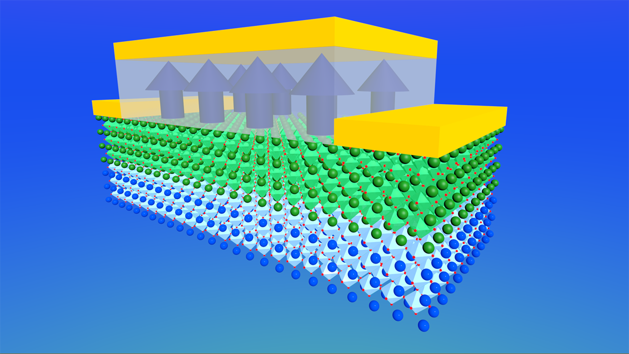
An atomic-scale rendering of the Mott insulator (green) and underlying material (blue) that proved key to refining and stabilizing the performance of a potentially smaller transistor.
The team had, in effect, kept the Jekyll and domesticated the Hyde. The space-saving benefits of the high-density region remained, but because the overall density had dropped (thanks to the additional, bottom layer), the team retained greater control over the insulator-metal transition, too. That advantage manifested in the form of a record-high on-off ratio, which came in at a whopping 385 — more than 20 times higher than any yet reported. That number, Hong said, may be scraping the ceiling of what can be reached with the Mott-ferroelectric approach.
Also in its favor? Ferroelectrics are non-volatile, meaning that they can retain their 1s and 0s without a constant power supply. And the fact that they require only sips of voltage to flip their polarization makes the Mott-ferroelectric pairing more energy-efficient than similarly non-volatile but magnetism-based memory, including MRAM.
“To me, in terms of technology development, it’s a big deal, because this shows that it is possible,” Hong said. “We can have very high-performance devices, retaining many manufacturing processes of conventional semiconductors and overcoming some fundamental limitations of them.”
To Hong’s mind, Mott-based transistors could wind up finding their way into those devices sooner than later.
“I think it’s ready,” she said of the concept. “It’s really competitive with other non-volatile memory technologies. I think someone who has the right mindset can pick up the concept and run with it.”
The team reported its findings in the journal Nature Communications. Hong, Hao and Chen authored the study with Nebraska’s Le Zhang, Brookhaven National Laboratory’s Yimei Zhu, Myung-Geun Han and Wei Wang, the University of the Basque Country’s Yue-Wen Fang, and NYU Shanghai’s Hanghui Chen. The researchers received support primarily from the U.S. National Science Foundation, which awarded Nebraska a $20 million grant in 2021, along with the Semiconductor Research Corporation.


