Electrical and Computer Engineering
Karl Vogel, October 18, 2023
Creating hybrids of defects, Sutters seek to ‘tune’ new avenues in nanowires
For decades, scientists working on semiconductors have believed defects are harmful to electronic materials. This is especially the case with dislocations, a class of imperfections that cause an abrupt change in the arrangement of atoms along a line in a crystal.
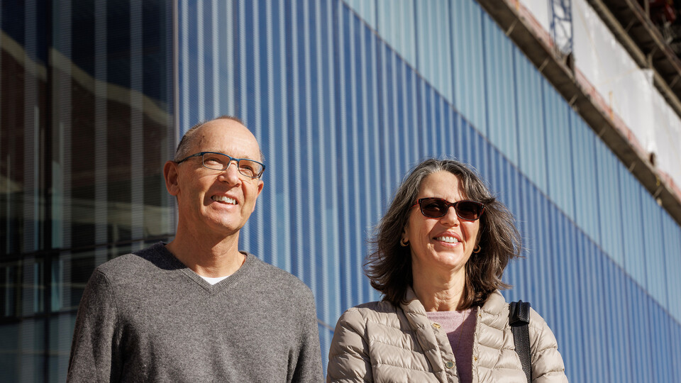
Research by Nebraska Engineering faculty Eli Sutter and Peter Sutter is setting the stage for challenging these long-held beliefs and, potentially, changing the fundamental perception of defects in electronic technology.
In an article published in the Journal of the American Chemical Society, the Sutters and Raymond Unocic from Oak Ridge National Lab outline their discovery of a materials synthesis method that can control the placement and types of dislocations that can optimize the specific advantages these imperfections offer. This discovery was made as part of a three-year, $520,000 project that was funded by the National Science Foundation Division of Materials Research.
“The new method allows us to control the positioning of a single defect in a semiconductor in a way that its whole volume experiences the defect. And we can now tune the characteristics of the defect with very high fidelity,” said Eli Sutter, professor of mechanical and materials engineering.
In semiconductors used in microelectronics, for example, dislocations are considered to “scatter” or impede the flow of electrons in devices such as transistors and to limit light emissions from the semiconductor.
The Sutters’ new synthesis method produces a hybrid of the two primary types of dislocations — screw and edge — in an ultra-thin semiconductor nanowire. The geometry of these dislocations could then be precisely adjusted (or “tuned”) to exploit the resulting new properties.
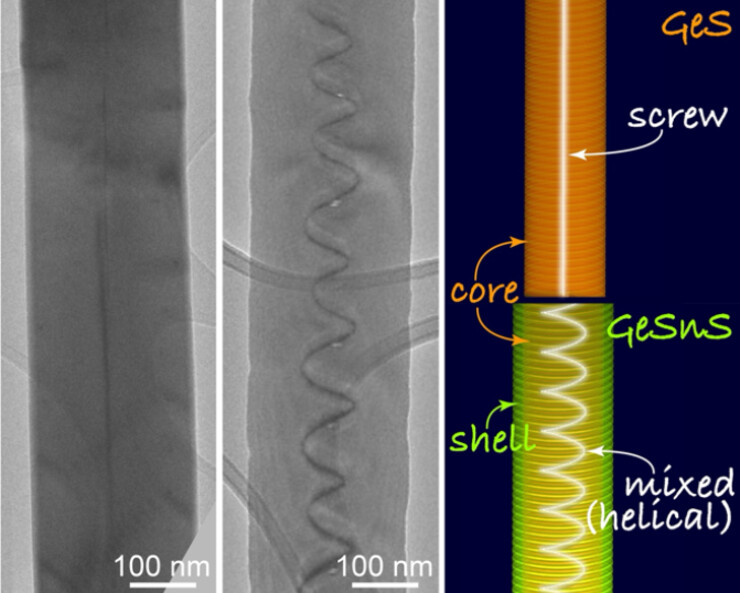
“What we show is not necessarily what properties come out, but how we can control the defect in the first place to explore these properties,” said Peter Sutter, professor of electrical and computer engineering. “Now, we not only control the positioning of a single defect, we can even kill the characteristics of the defect.”
Peter Sutter said screw and edge dislocations should, theoretically, have vastly different effects on electronic properties of semiconductors and could also have new and beneficial properties, such as being used in place of a thin-film semiconductor in some devices.
This new synthesis method, he said, also opens a pathway for research that could improve materials once thought to need pristine nanowires to be valuable.
This exploration will begin in the Sutters’ next project — a three-year, $542,870 DMR-funded project with Eli Sutter as principal investigator.
“We’re kind of picking up at the point where this paper leaves off,” Peter Sutter said.
Adopting a strategy used by plant scientists to create new lines of crops such as wheat and corn that are more resilient and successful in harsh environments, the Sutters will be looking to create hybrid semiconductor structures to open up new ways of controlling single defects.
“These hybrids, or heterostructures, offer great possibilities,” Peter Sutter said. “For example, they may allow us to seed tunable dislocations into other materials.”
The Sutters’ research on defects in semiconductor nanostructures is funded by the program on Solid State and Materials Chemistry within the Division of Materials research of the National Science Foundation.
Electrical and Computer Engineering Engineering Mechanical and Materials Engineering


