Mechanical and Materials Engineering
Scott Schrage, January 15, 2020
Nano-engineering technique could aid exploration, scalability of next-gen electronics
Just add sulfur.
Nebraska engineers Peter and Eli Sutter have shown that the elemental condiment can spice up a nanomaterial sandwich by putting a literal twist on the multi-layered classic.
That twist, a 30-degree rotation of each atomically thin layer relative to the one below it, could help enliven technological menus at five-star laboratories worldwide: emergent electronic or optical properties, greater speed, more functionality in less space.
After all, you’re my van der Waals
For the better part of a decade, engineers have been crafting and testing recipes for so-called van der Waals heterostructures: stacks of atomically thin crystal layers that can be sequenced just so. Compared with a homostructure — the nanoscopic equivalent of a slab of ham — a heterostructure might feature slices of pastrami, pepperoni and pepper jack, all held together by the weak van der Waals forces among neighboring atomic layers.
“This stacking opens up many possibilities, because it allows us to mix and match a vast library of available materials,” said Peter, professor of electrical and computer engineering.
Engineers soon discovered that the diversity could cultivate technologically interesting properties, often in the regions where two different materials meet, that are otherwise difficult or impossible to recreate. Then, a few years ago, researchers began exploring the effects of rotating the layers within van der Waals stacks. That misalignment of layers, they found, could also yield interesting results — turning a material into a superconductor, for instance, or changing how a semiconductor emits light.
Yet the achievement came in the face of a considerable challenge: Despite the weakness of van der Waals forces, adjacent layers strongly prefer to remain aligned. Manually stacking layers one by one can overcome the issue but demands extreme precision and, more importantly, time that large-scale manufacturers of small-scale technology just don’t have.

“It’s not scalable in any (meaningful) way,” said Eli, professor of mechanical and materials engineering. “If one wants to develop applications based on twisted van der Waals stacks, it is impossible to imagine factory workers sitting there and arranging these pieces, by hand, on top of one another.
“One has to manually stack one little flake at a time. To build one device, maybe that can work. To build 10, maybe it’s (just) tedious. But more than that is definitely out of reach.”
So the Sutters, alongside colleagues from Aalto University and the University of Wyoming, decided to try a different tactic: directly synthesizing twisted stacks. Managing that, though, meant overcoming a foundational principle of thin-film growth: the tendency for each added layer to inherit its orientation from the underlying crystal.
“We thought that if we could first grow some other crystal that would then be transformed into the desired one, then maybe this intermediate crystal, rather than the underlying substrate, could dictate the orientation of the final product,” Peter said.
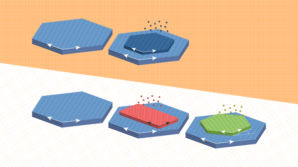
They started with a support of tin disulfide, a compound that features two sulfur atoms for every tin atom and is useful as a layered semiconductor. After growing an atomically thin layer of tin monosulfide — one sulfur atom, one tin — on the tin disulfide base, the team saturated that tin monosulfide with a sulfur vapor.
As expected, the tin monosulfide spontaneously transformed into tin disulfide. But because tin monosulfide crystals grow in a rectangular lattice — as opposed to the hexagonal configuration of tin disulfide — the lattice of the newly transformed second layer adopted a 30-degree twist relative to the supporting crystal. And when the researchers repeated the process, the third layer took its cue from the second, rotating 30 degrees relative to it and 60 degrees relative to the first.
To demonstrate the generalizability of the approach, the team achieved the same feat after replacing the tin disulfide substrate with two other van der Waals semiconductors, molybdenum disulfide and tungsten disulfide.
Next-generation gap
Twisted heterostructures are showing particular promise for modifying an essential aspect of atomically thin semiconductors: their bandgaps. The electrons in semiconductors each possess a certain amount of energy — within a range of distinct energy values called the valence band — when left undisturbed. When excited by heat or light, those electrons jump to a range of higher energy values — the conduction band — that allows them to flow as electricity. The gap between those two bands, or bandgap, helps dictate how semiconductor materials conduct electric current and absorb or emit light.
“So some very interesting properties can emerge if you play this twisting game,” Peter said.
The same twisting that could inform next-generation micro- and opto-electronics also evokes the mosaics of ancient Rome and Islam, he said, creating a quasi-crystalline tiling pattern that fills space not by periodically repeating the same basic unit, as ordinary crystals do, but by yielding multiple complementary shapes.
Though that twisting represents a victory over the van der Waals tendency toward alignment, Peter said, mastering twisted heterostructures still presents formidable challenges.
“It’s a start,” he said of the team’s progress. “It’s not fully satisfactory yet, because we cannot, for example, (choose) the twist angle that we want.
“But at least it’s no longer zero degrees.”
The team, which reported its findings in the journal Nature Communications, received support from the U.S Department of Energy’s Office of Science and the Academy of Finland.


